Tutorial: Designing a Mach–Zehnder Interferometer
This is a hands-on walkthrough, written the way a photonic circuit designer actually thinks while laying out a chip. Together we will build one of the most important building blocks in integrated photonics, a Mach–Zehnder interferometer (MZI), taking it from a blank canvas to an exported GDS. Along the way you will touch nearly every feature of Phidler.
If you have never opened the app before, skim the User Guide first to get the lay of the land. This page assumes you already know where the panels are, so it focuses on designing something real.
What we are building, and why
A Mach–Zehnder interferometer splits light into two paths ("arms"), lets the two halves travel different optical path lengths, and then recombines them. The recombined intensity depends on the phase difference the two arms accumulated, which in turn depends on wavelength. That makes the MZI the workhorse behind:
- Modulators. Put a phase shifter on one arm and you can switch light on and off.
- Filters / (de)multiplexers. An imbalanced MZI (one arm physically longer than the other) is wavelength-selective, with a periodic transfer function.
- Sensors. Anything that changes the index in one arm shows up as a phase shift at the output.
We will build the imbalanced version, because that length difference is exactly what Phidler's goal-length routing was made for.
A quick bit of physics so the numbers later mean something. The phase a guided
mode accumulates over a physical length L is
phase = (2π / λ) · n_eff · L
where n_eff is the waveguide's effective index. The two arms interfere
constructively or destructively depending on their phase difference,
Δphase = (2π / λ) · n_eff · ΔL, where ΔL is the path-length imbalance.
The output is periodic in optical frequency, and the period (the free spectral
range, or FSR) is set by that imbalance:
FSR ≈ c / (n_g · ΔL)
(n_g is the group index). So the single most important number we will dial in
is ΔL, the extra length of one arm. Keep that in mind. It is the reason we
ask Phidler to route one arm to a specific target length.
Step 1 — Start a project and pick a platform
When Phidler launches (or on File → New) it asks what material platform you are designing for. This is not cosmetic: the core/cladding indices and the design wavelength feed the suggested single-mode waveguide width, the propagation-time readouts, and the FDTD simulator later.
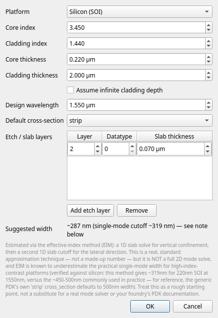
For this tutorial pick Silicon (SOI) at 1550 nm, the standard telecom-band silicon photonics platform. Notice the dialog suggests a single-mode width (around 450–500 nm is typical for 220 nm SOI strip; the tool's effective-index estimate runs a little narrower and says so). Accept the defaults and continue.
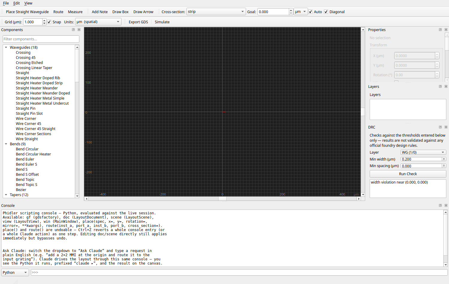
You are now looking at the main workspace: the component palette on the left, the canvas in the middle, Properties / Layers / DRC docks on the right, and a scripting Console along the bottom.
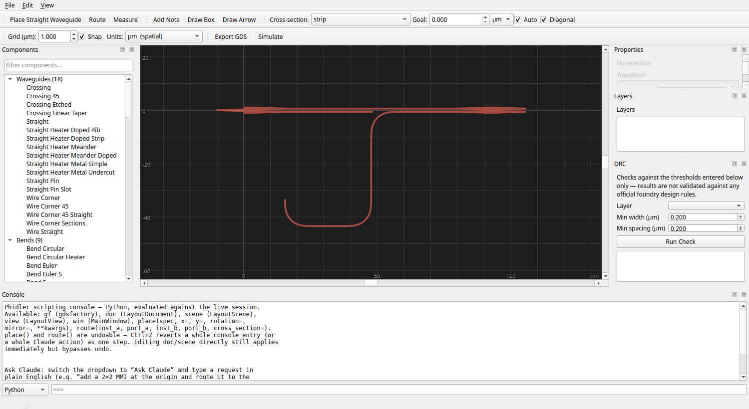
Tip: Everything in the View menu is yours to rearrange. You can hide any dock, and toggle the inline component thumbnails in the palette if you prefer a denser text-only list.
Step 2 — Place the splitter and the combiner
An MZI needs a 1×2 splitter at the input and a 2×2 (or 2×1) combiner at the output. Silicon photonics almost always uses multimode interference (MMI) couplers for this. They are compact, broadband, and fabrication-tolerant.
- In the palette, open Couplers → MMIs (or just type
mmiinto the filter box at the top of the palette). Hovering a component shows a live preview of its geometry. - Click
mmi1x2to arm it, then click on the canvas to drop it. This is our splitter: one input port (o1) on the left, two outputs (o2,o3) on the right. - Click
mmi2x2and place it to the right of the splitter. This is our combiner: two inputs (o1,o2) on the left, two outputs (o3,o4) on the right. The second output is what makes the interference measurable. In a real chip you would send each output to a photodetector.
Select the combiner and use the Properties panel to set its exact position (say X = 90 µm) so there is room for the arms to breathe. You can also drag it; with snapping on, it will grid-align as you move, and the snap now happens live while you drag, not just when you let go.
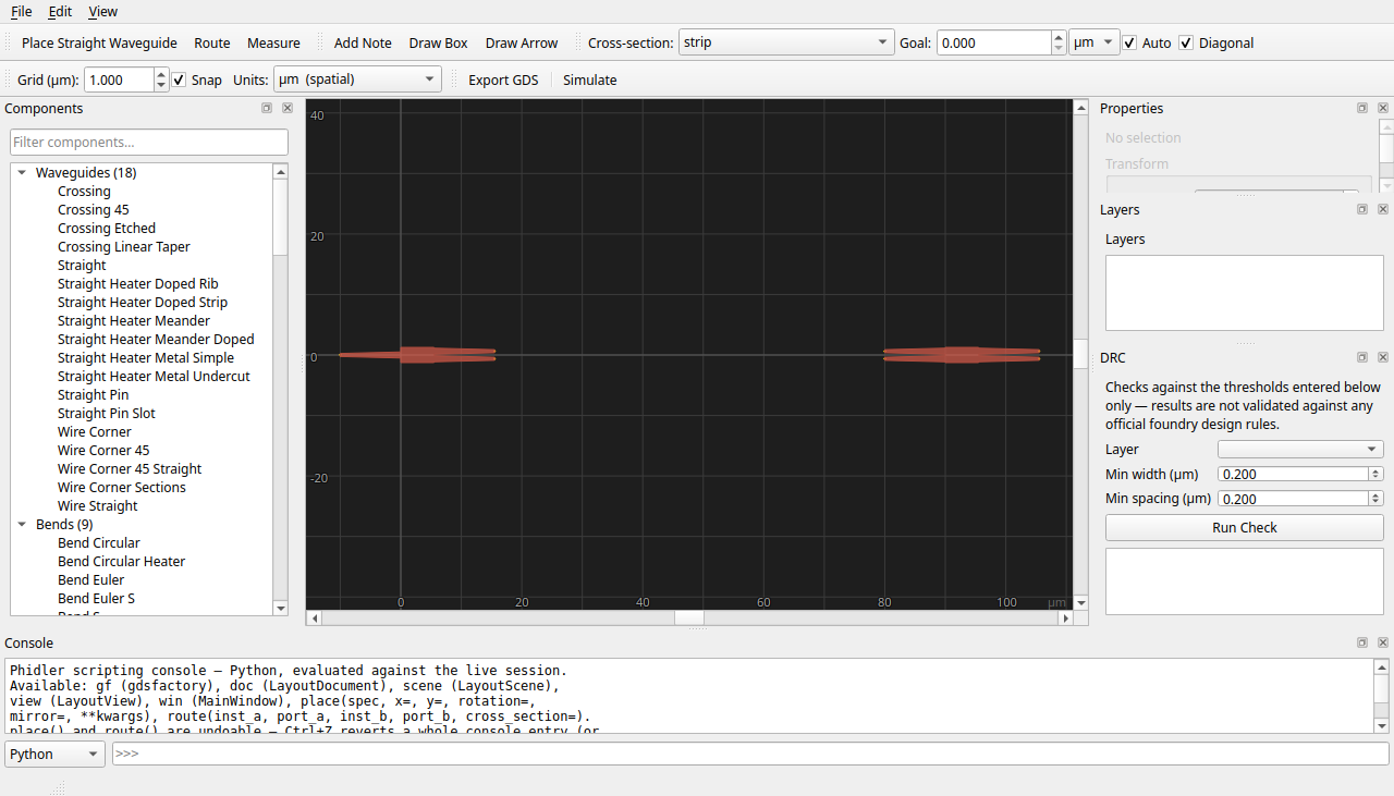
Orientation matters. The combiner's input ports face left (west) and the splitter's outputs face right (east), so they naturally face each other. If you ever place a component the wrong way round, use Edit → Flip Horizontal (
H) or Flip Vertical (V) to mirror it about either screen axis.
Step 3 — Route the first (reference) arm
Now we connect ports with real waveguides. Click Route in the toolbar (or press the routing toggle) to enter routing mode. The cursor becomes a crosshair.
As you move over the layout, Phidler highlights the port you would snap to
with a cyan ring, so you never have to pixel-hunt for a 0.5 µm-wide waveguide
tip. Click the splitter's top output (o2). A rubber-band preview track now
follows your cursor from that first port, and the next port you hover is
highlighted, so you can see exactly what you are about to connect before you
commit.
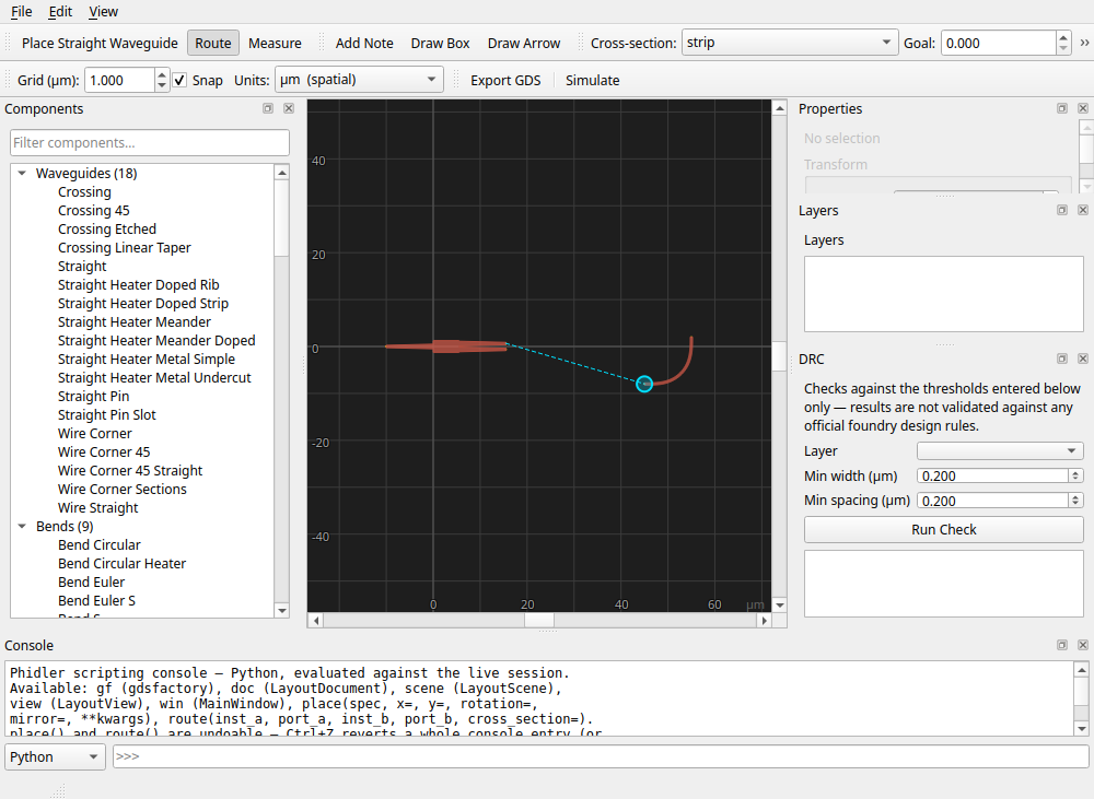
Click the combiner's top input (o2) to finish the route. Phidler runs a real
gdsfactory router and lays down a waveguide with adiabatic Euler bends (the
low-loss bend shape that gradually changes curvature rather than snapping to a
fixed radius). This is our reference arm. We let it take the shortest
natural path.
Step 4 — Route the second arm to a target length (the delay)
Here is the heart of an imbalanced MZI. The lower arm needs to be longer
than the reference arm by a controlled amount, ΔL, to set the filter's
free spectral range.
Before drawing the second arm, set a length goal in the routing toolbar:
- Type a target into the Goal field. For this design, set 140 µm (the natural path is only ~55 µm, so this asks for a healthy delay).
- Leave the unit as µm. You could instead choose fs or ns and specify the delay in propagation time. Phidler converts it to a length using the current effective index, because for a delay line what you usually care about is picoseconds, not microns.
- Make sure Auto is checked. In automatic mode, Phidler inserts an adiabatic meander and binary-searches the meander size until the routed length lands on your target (to within a fraction of a micron). With Auto off (manual mode) it routes directly and simply reports how far you are from the goal, leaving the adjusting to you.
Now route the splitter's lower output (o3) to the combiner's lower input
(o1). Watch the lower arm come in as a meander. That serpentine is the extra
optical path, built from the same low-loss Euler bends.
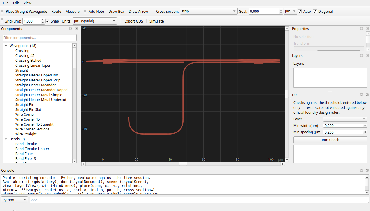
You have just built a complete, imbalanced Mach–Zehnder interferometer: one straight reference arm, one length-matched delay arm, between an MMI splitter and an MMI combiner.
Step 5 — Read back length and propagation time
Select the delay arm (click it once, with routing mode off). The status bar reports the route's physical length, the propagation time that length implies at the current effective index, and (because we gave it a goal) the target and the delta from it, plus whether the match was automatic or manual.
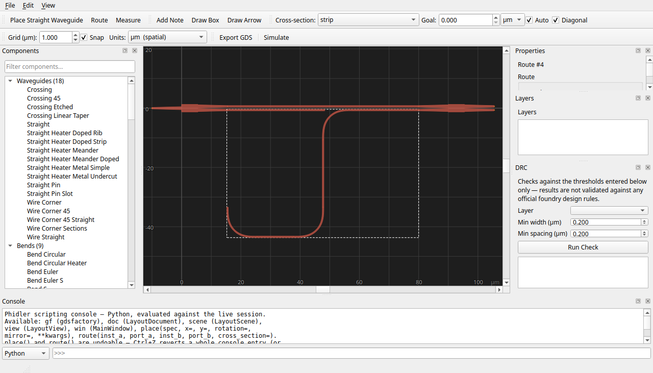
This is where the design choices become physics. With ΔL now fixed by
the two arms' lengths, you can sanity-check your free spectral range against the
formula above. If the FSR is wrong, change the Goal and re-route the arm.
The meander resizes to match.
Switching the whole canvas to time units. The toolbar Units selector flips every coordinate readout between spatial (µm / nm) and propagation time (fs / ns). In time mode the rulers and cursor readout show how long light takes to traverse a distance, using the effective index from your last mode solve (or the core index if you have not run one). For delay-line work, designing directly in femtoseconds is often more natural than in microns.
Step 6 — Check the guided mode and simulate
Before trusting any layout, a photonic designer confirms the waveguide actually guides a single, well-confined mode. Open the FDTD simulation window from the Simulate button in the toolbar.
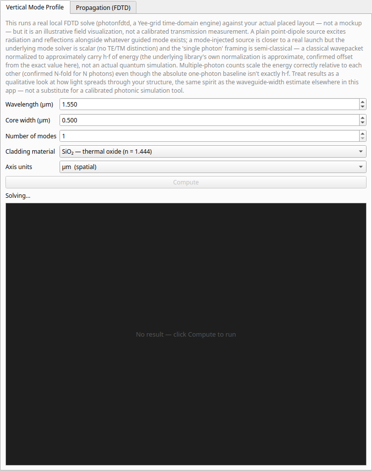
The Vertical Mode Profile tab solves the waveguide cross-section and shows the mode and its effective index. The core is outlined in cyan over the field, so you can see at a glance how the mode sits relative to the waveguide. A well-confined mode sits comfortably inside that outline; if the cladding is too thin the solver warns that the mode is truncating against the domain edge. (If you want to model an unbounded stack, the Project Settings "assume infinite cladding depth" option sizes the cladding generously so confinement is never artificially limited.)
The Propagation tab runs a true 3-D FDTD time-domain simulation: place a source, hit Compute, and watch the field animate down the guide. Here too the circuit elements are outlined in cyan on top of the field, so you can read where light is relative to your structures rather than guessing.
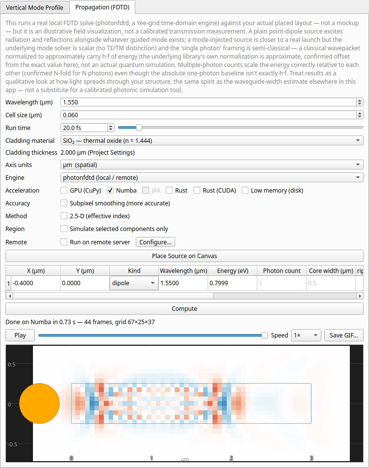
You choose the excitation per source in the source table's Kind column:
- dipole. A plain oscillating point source; always available.
- single photon. Launches the locally-solved guided mode (a mode-matched source).
- scripted. Drives the source with your own Python waveform expression.
- cherenkov. Models a charged particle punching up through the chip (perpendicular to the layout, out of the top-down view) faster than light's local phase velocity, laid down as a track of time-staggered dipoles along the z axis (transit time = distance / βc). Their superposition forms the Cherenkov shock cone, seen top-down as a ring spreading from the impact point. Set the particle speed (β = v/c) and the tilt from vertical in the source row.
The effective index your mode solve produces is fed back into the propagation time readouts and rulers, so after solving, the femtosecond numbers on your delay arm reflect the real mode, not just the bulk material index.
Step 7 — Run a quick design-rule check
Foundries impose minimum widths and spacings. Open the DRC panel, enter the thresholds for your process, and run the check. Violations are highlighted on the canvas in red, and double-clicking one jumps the view straight to it.
For our MZI the thing to watch is the meander: tight delay lines can pull waveguides close enough to couple unintentionally. If the DRC flags a spacing violation in the serpentine, give the arm a larger goal length (more room to spread out) or move the components farther apart and re-route.
Step 8 — Export
When the layout passes, export it:
- File → Export GDS… writes the flattened mask layout you would hand to a foundry. Routes, components, and arrays all come through as real geometry.
- File → Export Python Script… writes a standalone gdsfactory script that recreates the design as reviewable, version-controllable code.
- File → Save keeps the editable
.phidlerproject, which remembers everything, including each route's length goal, so reopening reproduces the exact same meander.
Where to go next
You now have the full loop: place, route, length-match, verify, and export. A few natural extensions of this same MZI:
- Make it a modulator by leaving room on one arm for a phase shifter, and arraying contact pads with the Array options in the Properties panel (columns / rows / pitch) instead of hunting for a pre-made pad-array part.
- Build a filter bank by duplicating the MZI with different delay lengths. Each goal length you type sets a different free spectral range.
- Tune for fabrication by sweeping the waveguide width in Properties and re-checking the mode profile.
For the full reference on every panel and tool, see the User Guide. For how the app is built and tested, see Development.