User Guide
Phidler is a graphical layout tool for photonic integrated circuits, built on gdsfactory and its generic PDK. You place real photonic components, wire them together with real routed waveguides, check the result, and export a foundry-ready GDS. No code required, though Python is always a keystroke away (and if you'd rather not touch either, you can just ask Claude; see Ask Claude to build it).
This page is the reference: every panel and every tool, in depth. If you'd rather learn by building something concrete, the MZI tutorial walks the whole flow end to end on a real device.
The design process, end to end
A photonic layout comes together in roughly this order. Each phase feeds the next, so it helps to see the whole arc before diving into the details:
- Pick a platform (Project Settings). The material system (silicon, silicon nitride, lithium niobate/tantalate) sets the core/cladding indices and thickness that drive the suggested waveguide width, the propagation-time readouts, and the FDTD stack. Choose this first: it is the physical context everything else is interpreted in (and it is reopenable anytime).
- Place components (Placing components). Drop the building blocks of your circuit (splitters, bends, rings, grating couplers) from the palette. Phidler exposes ~300 components from the generic PDK, grouped by function. This is choosing what sits on the chip.
- Set each component's parameters (Editing parameters). Dial in lengths, widths, radii, gaps, and the cross-section each part uses. The cross-section is the most consequential choice. It decides the waveguide's width and which layers the geometry lands on, and it is what lets a component connect cleanly to the rest of your circuit.
- Connect them with routes (Routing). Click port-to-port and Phidler lays down a real waveguide with low-loss Euler bends, optionally length-matched to a target delay. This is where a set of parts becomes a circuit.
- Verify. Two independent checks: DRC for geometric rules (minimum width/spacing), and FDTD simulation for the physics. First a sub-second vertical mode solve to confirm the waveguide guides a single, well-confined mode, then full 3D propagation to watch light move through the device. The mode solve's effective index feeds back into the propagation-time readouts, so verifying and designing inform each other.
- Export (Saving, loading, and exporting).
A
.phidlerproject to keep editing, a.gdsfor the foundry, or a gdsfactory.pyscript for code review and version control.
In practice you won't go straight down the list. You'll route, hit a spacing violation, widen a gap, re-route, re-simulate. The point is that the tools are arranged around that loop. The rest of this guide covers each phase in turn.
Project Settings
On startup (and via File > New), Phidler shows a Project Settings dialog:

- Platform: pick Silicon (SOI), Silicon Nitride, Lithium Niobate (LN), Lithium Tantalate (LT), or Custom to set the core/cladding refractive indices and core thickness. LN/LT use real published thin-film-on- insulator index values (cross-checked against literature; see Development for sourcing), not a full multi-layer stack-up model. There's no LN/LT-specific cross_section in the generic PDK either, so these presets affect the suggested-width estimate and project metadata, same as the other platforms, not the actual GDS layers.
- Design wavelength: used together with the platform to estimate a suggested single-mode waveguide width.
- Cladding thickness: a generic default (2µm), not tied to any specific foundry process or platform. Switching platforms doesn't change this field, since it's a wafer/process choice rather than a material property. It doesn't affect the suggested-width estimate (which assumes a semi-infinite cladding) but is the real vertical extent used by FDTD Simulation's mode solver and propagation runs; see FDTD simulation for why this number actually matters there.
- Default cross-section: which gdsfactory cross-section new routes use by default.
- Etch / slab layers: for rib waveguides, list the partial-etch layers (e.g. SLAB150 on layer 2) and the slab thickness each leaves behind: the core height remaining after the etch, less than the full core thickness above. FDTD Simulation then models a ridge-over-slab rib instead of a fully etched strip (see FDTD simulation). Leave it empty for a plain strip waveguide. Add a row with Add etch layer; a row left at 0 µm is ignored.
The suggested width is an estimate from the effective-index method, not a full 2D mode solve. Read the note in the dialog before treating it as exact. It's a starting point, not a substitute for your foundry's PDK documentation.
You can reopen this dialog anytime via File > Project Settings… without clearing your current design.
Placing components
Use the Components panel on the left:
- Type in the filter box to search by name.
- Core photonics categories (waveguides, bends, couplers, MMIs, rings, MZIs, grating couplers, filters, spirals, tapers, edge couplers, detectors) are expanded by default. Everything else (MEMS, quantum, microfluidics, analog, test structures, etc.) is under Other.
- Hover over a component to preview its actual geometry before placing it.
- Click a component (or select it and press Enter) to arm placement, then click on the canvas to place it.


The component catalog
Phidler exposes the placeable parts of the generic PDK, roughly 300 components that build cleanly on their own. (Parts that need required arguments, or that are not real standalone cells, are filtered out so everything in the palette actually places.) They are grouped by function; the core photonic categories are expanded by default, and each one answers a recurring need in a circuit:

- Waveguides: the straight sections (and crossings) light travels along.
straightis the workhorse;crossinglets two waveguides cross with low crosstalk;straight_heater_metal_simplecarries a heater on top for thermo-optic tuning, andstraight_pinembeds a PIN junction for modulation. - Bends turn a waveguide.
bend_euleris the default low-loss adiabatic bend (curvature ramps up gradually rather than snapping to a fixed radius);bend_circularis a constant-radius turn;bend_sandbezieroffset a waveguide sideways. - Tapers smoothly change a waveguide's width or cross-section.
taperis linear;taper_adiabaticandtaper_parabolicare lower-loss profiles;taper_sc_nc/taper_nc_scconvert between silicon and nitride waveguides. - Couplers split or combine light by evanescent coupling between two
closely-spaced waveguides.
coupleris a directional coupler;coupler_ringcouples a bus into a ring;coupler_adiabaticandcoupler_broadbandsplit flatly across wavelength. - Edge couplers get light on and off the chip at a cleaved facet:
edge_coupler_silicon, oredge_coupler_arrayfor a whole fiber array. - MMIs are multimode-interference splitters, the compact, broadband,
fabrication-tolerant workhorse for splitting and combining:
mmi1x2(1→2),mmi2x2(2→2), plus_with_sbendvariants that fan the ports apart. - Rings are resonators for filtering, modulation, and sensing:
ring_single,ring_double,ring_single_pn(a modulator),ring_double_heater(tunable), anddisk(a whispering-gallery disk resonator). - MZIs are ready-made Mach–Zehnder interferometers (the tutorial
builds one by hand from MMIs and routes):
mzi, andmzi_latticefor a cascade with a sharper filter response. - Grating couplers couple light vertically to a fiber above the chip via
a diffraction grating:
grating_coupler_elliptical_te,grating_coupler_rectangular,grating_coupler_array. - Filters are wavelength- and polarization-selective parts:
dbr(a Bragg reflector),awg(an arrayed-waveguide-grating (de)multiplexer),polarization_splitter_rotator, andterminator(dumps unwanted light without reflecting it). - Spirals coil a long waveguide into a small footprint, for delay lines or
on-chip propagation-loss measurement:
spiral,delay_snake,spiral_racetrack_heater_metal. - Detectors:
ge_detector_straight_si_contacts, a germanium photodetector that converts guided light into photocurrent.
Everything else (MEMS, quantum/superconducting parts, microfluidics, analog RF, pads, vias, dies, text, and process-control test structures) lives under Other. Use the filter box to search across all of them by name (it matches both the raw gdsfactory name and the prettified display label).
Custom components
File > Import Custom Components… loads a Python file and adds any
@gf.cell-decorated functions it defines (with no required arguments) to
the palette under Custom. The file is remembered with the project, so
reopening a saved project that uses a custom part re-imports it
automatically.
Editing on the canvas
- Select: click an item. Rubber-band drag to select multiple, or
Edit > Select All (
Ctrl+A). The rubber band works like KiCad: drag left → right to select only items the box fully encloses (a window select), or right → left to also grab anything the box merely touches (a crossing select). The status bar names the mode as you drag. To reach an item buried under others, Alt+click cycles down through the stack, or right-click and pick it from Select under cursor. - Move: drag a selected item. Dragging a port close to another instance's port snaps them into exact alignment; otherwise the move snaps to the grid. Snapping is applied live as you drag, not just on drop.
- Rotate / Flip:
Rrotates 90°;HandVflip the selection horizontally / vertically (about either screen axis). You can also use the on-canvas transform overlay (see below). - Delete / Copy / Paste:
Delete,Ctrl+C,Ctrl+V. - Cancel with
Esc: backs out of whatever you're in the middle of: an armed placement, the measure, source or probe tool, or a route.Escworks no matter which panel has focus (you don't have to click the canvas first). Routing is two-stage: the firstEscdrops a half-finished route (the start port you picked), and a secondEscexits routing mode. - Undo / Redo:
Ctrl+Z/Ctrl+Shift+Z. - Pan: middle-mouse-drag. Zoom: scroll wheel, or View > Zoom to
Fit / Zoom to Selection (
Ctrl+0/Ctrl+Shift+0). - Right-click the canvas for a context menu of common actions.
- Grid pitch and snap-to-grid are adjustable from the toolbar.
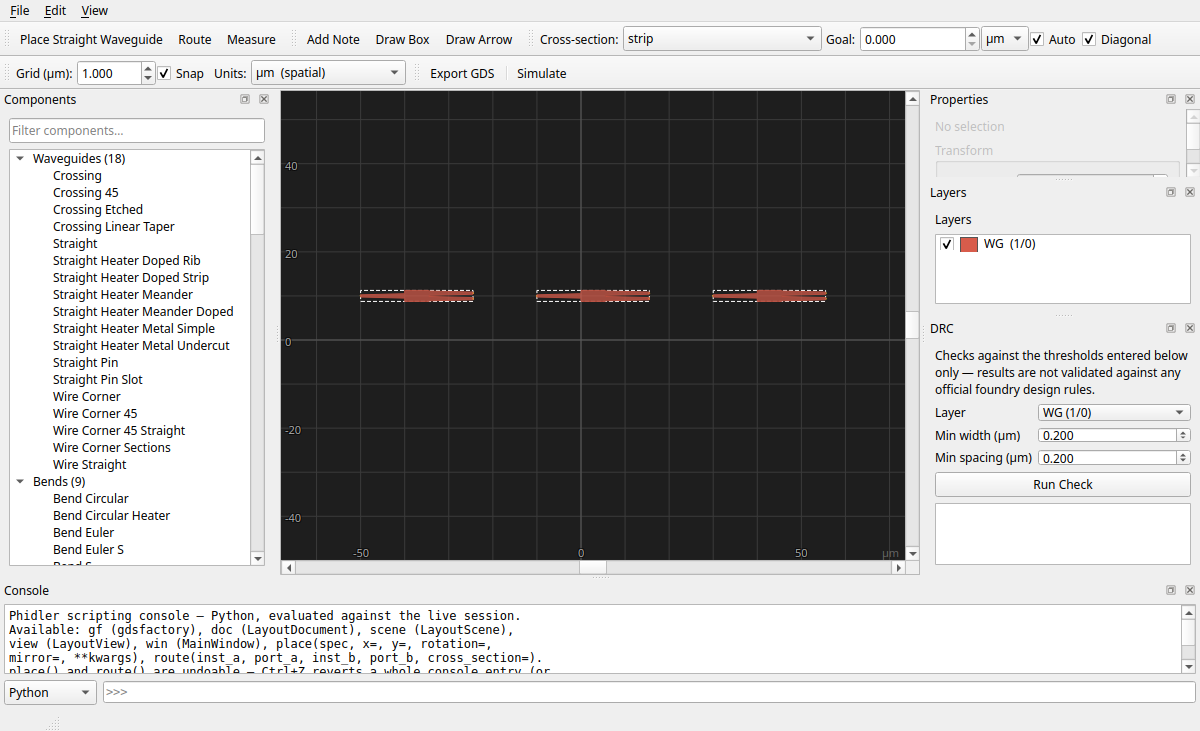
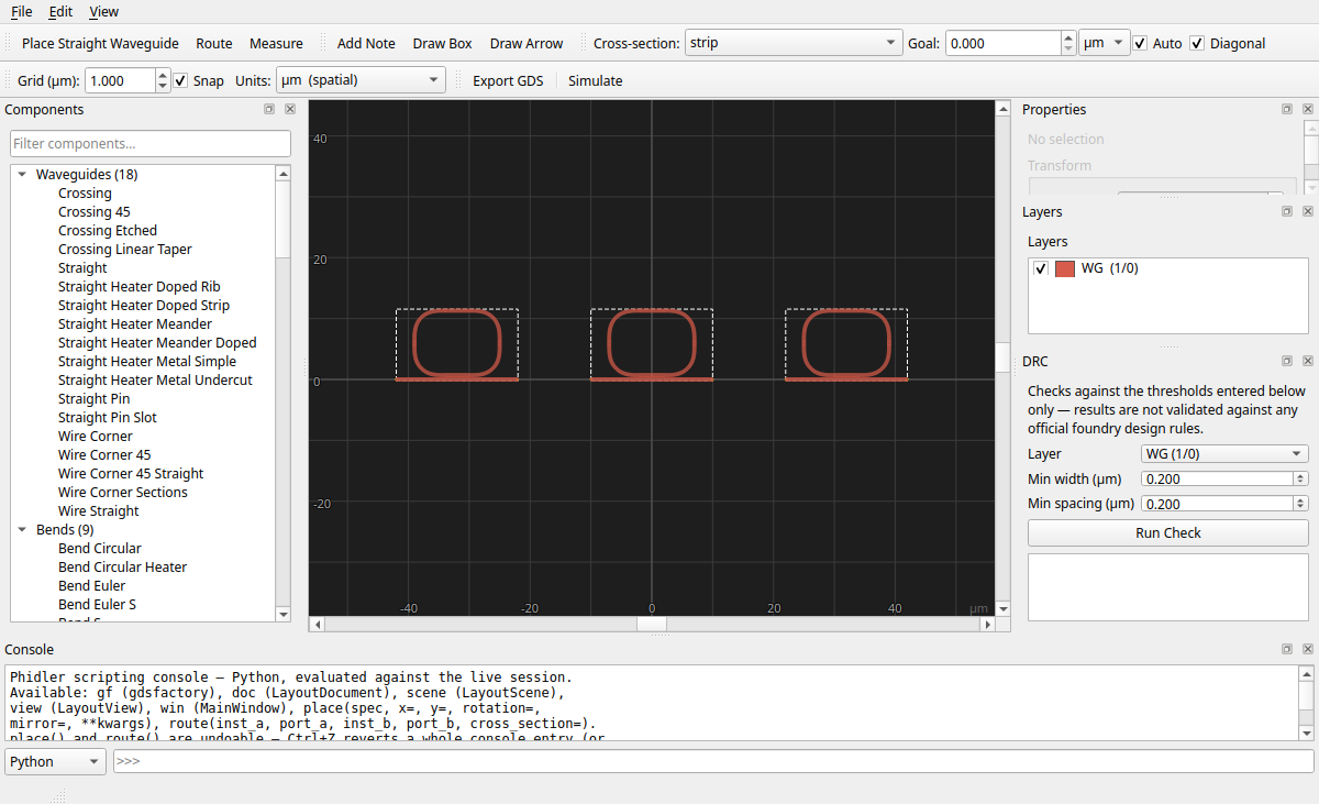
Aligning and distributing multiple instances
Select 2 or more instances, then use Edit > Align (or the same submenu in the right-click context menu):
- Align Left/Right/Top/Bottom Edges, or Align Horizontal/Vertical Centers.
- Distribute Horizontally/Vertically: needs 3+ instances; spaces their centers evenly along that axis, keeping the two extreme instances fixed.
Each is a single undo step, even when it moves several instances.
Transform handles
Selecting a single instance shows a rotate handle above it on the canvas:

- Drag the handle above the shape to rotate freely around the instance's position. It previews live and commits to the undo stack on release.
- For a quick 90° rotation, a flip, or resetting rotation/mirror/scale back to
defaults, use
R/H/Vor the right-click context menu. - Scale is not a drag gesture. Set it numerically in the Properties panel's Scale field (below), so a stray drag can't accidentally resize a component. Scale is a real geometric magnification of the shape and ports, not a component parameter like length.
Editing parameters
Select an instance and use the Properties panel (right side) to edit
its parameters: length, width, radius, cross-section, etc. Click Apply
to regenerate its geometry. cross_section is a dropdown of the active
platform's valid names, so you can't type something invalid.

What the parameters are, and how they edit
Phidler reads the component's actual function signature, so the fields you see are exactly the parameters that part accepts. They differ from component to component. Every parameter that has a default is shown, and how it edits depends on its type:
- Numbers (lengths, widths, counts, radii) are numeric fields.
- Booleans are checkboxes.
cross_sectionis a dropdown constrained to the active PDK's valid names, so you cannot type one that will not build.- Other text parameters are free-text fields. A few take the name of a
sub-component (e.g.
bend="bend_euler"); these are editable, but most designs leave them at the default. - A parameter whose default is a complex object (a function, a list) is shown greyed-out with its value and marked "not editable from the panel yet". Adjust those by exporting to a script or from the console instead.
Click Apply to rebuild the instance's geometry from the new values (undoable like any edit). The parameters you will meet most often, across many components:
| Parameter | What it controls |
|---|---|
cross_section |
The waveguide profile — width and layers — the part is drawn with. The most consequential parameter; see below. |
length |
Length of a straight section, taper, or heater (µm). |
width |
Waveguide or feature width (µm). Widening raises confinement and shifts the effective index. |
radius |
Bend radius (µm). Smaller is more compact but lossier, down to a minimum the cross-section enforces. |
gap |
Edge-to-edge spacing (µm) between two coupled waveguides (couplers, rings) — the single biggest lever on how strongly they exchange light. |
length_x / length_y |
The footprint of a two-dimensional part — an MZI's arm length, a ring's straight sections. |
npoints |
How many points discretize a curve: higher is smoother but heavier geometry. |
taper_length |
The length a width/cross-section transition happens over; longer is more adiabatic (lower loss). |
spacing / pitch |
Center-to-center spacing in arrayed parts (grating-coupler arrays, edge-coupler arrays). |
Cross-sections
A cross-section is the recipe for a waveguide's transverse profile: its
width, and which layers it occupies. It is both a component parameter
(cross_section) and the choice in the routing toolbar, so a route and the
components it joins can share one and line up. The generic PDK's main
cross-sections:
| Cross-section | What it is |
|---|---|
strip |
The default silicon wire — full-etch WG core, ~500 nm wide. Highest confinement; the standard for dense routing. |
rib / rib2 |
A ridge over a partial-etch slab (WG + SLAB). Lower loss and the basis for doped/active devices, at the cost of weaker lateral confinement. Tell the simulator about the slab so it models the rib correctly — see Rib waveguides. |
nitride |
A silicon-nitride (WGN) waveguide — lower index contrast means lower loss and broader bandwidth; used for visible light and low-loss interconnect. |
slot |
Two rails separated by a narrow gap that concentrates the field in the slot — for sensing and electro-optic/nonlinear fills. |
pn / pin |
A waveguide with a PN or PIN junction across it (adds doping layers) — the basis of carrier-depletion / injection modulators. |
strip_heater_metal / rib_heater_doped |
A waveguide with a heater on top (metal) or doped into the slab, for thermo-optic phase tuning. |
metal1 / metal2 / metal3 / metal_routing |
Not optical — electrical routing on the metal layers, for the contacts and pads active devices need. |
Because the cross-section decides which layers geometry lands on, your choice
here is what populates the Layers panel: picking rib, a pn, or a
heater cross-section is exactly what makes the slab, doping, and metal layers
appear.
Precision transform entry
The same panel has a Transform section above the parameter form: X, Y, Rotation, Mirror, and Scale as typed numeric fields, for exact placement instead of dragging by eye (matching a known coordinate from a foundry PDK, for instance). Edit the values and click Apply Transform to commit. It's undoable the same way a canvas drag is. The fields track the selected instance's live transform automatically; editing one pauses that tracking until you click elsewhere, so your typing isn't overwritten.
Layers
Every shape in a GDS layout lives on a layer, a (layer number, datatype)
pair that tells the foundry which fabrication step draws it: which etch, which
implant, which metal. A photonic component is rarely a single layer; a modulator,
for instance, carries a waveguide core, doping implants, contacts, and metal all
at once.
The Layers panel (right side) lists every layer your design actually uses.
It starts empty and grows as you place, route, and import. A layer appears the
moment some component puts geometry on it, named from the active PDK (WG,
SLAB150, M1, …). Toggle a layer's visibility or change its color with the
checkbox and swatch; hover a layer for a one-line note on what it is for (the
same descriptions collected below).

Layers appear because components carry them, not because you draw on them directly. Phidler routes optical waveguides; it has no electrical-net router, so the doping, metal, and heater layers below show up when you place a part that already includes them (a heater-tuned ring, a PN modulator, a detector) or pick a cross-section that uses them, not from wiring them yourself.
Layer types in the generic PDK
The generic PDK models a fairly complete silicon-photonics process. Grouped by what they do, these are the layers you are likely to encounter:
Silicon waveguide and etch: the layers that define where light is guided.
| Layer | What it is |
|---|---|
WG |
Silicon waveguide core — full etch (~220 nm on standard SOI). Defines single-mode wire waveguides and grating teeth. |
SLAB150 |
Half-etch silicon slab (~150 nm etch, leaving ~70 nm slab). Used under grating couplers and rib waveguides to improve coupling efficiency and confinement. |
SLAB90 |
Shallow-etch slab (~90 nm). For very-low-loss rib waveguides, where a thicker slab reduces scattering. |
SHALLOW_ETCH / DEEP_ETCH |
Process masks for the shallow (~90 nm) and full-depth (~220 nm) silicon etch steps. |
DEEPTRENCH |
Deep isolation trench etched through the whole device layer to isolate regions optically and electrically. |
UNDERCUT |
Removes buried oxide beneath the silicon to form suspended membranes — MEMS, or ultra-low-loss waveguides. |
WGCLAD |
Waveguide cladding (typically SiO₂) surrounding the core. |
The half-etch slab layers are exactly what FDTD's rib-waveguide support needs to know about to simulate a rib correctly rather than as a fully-etched strip.
Doping implants define PN/PIN junctions for modulators and the low-resistance contacts that feed them.
| Layer | What it is |
|---|---|
N / P |
Moderate n-type / p-type silicon doping — the junction of a PN-junction phase shifter or PIN modulator. |
NP / PP |
N+ / P+ implants — higher doping next to the waveguide to reduce series resistance. |
NPP / PPP |
N++ / P++ implants — heavy doping for low-resistance ohmic contact to metal vias. |
Germanium: for detectors and electro-absorption modulators.
| Layer | What it is |
|---|---|
GE |
Germanium grown selectively on silicon; absorbs near-IR (1.3–1.6 µm) for photodetectors and EA modulators. |
GEN / GEP |
N-doped / P-doped germanium — the cathode and anode contact regions of a Ge photodetector. |
Silicon nitride: a lower-contrast, lower-loss guiding layer.
| Layer | What it is |
|---|---|
WGN |
Silicon-nitride (Si₃N₄) waveguide core — lower index contrast than silicon gives lower loss and broader bandwidth; used for visible-light and low-loss interconnect PICs. |
WGN_CLAD |
Silicon-nitride waveguide cladding. |
Metals, vias, and heaters: electrical contact, routing, and thermo-optic tuning.
| Layer | What it is |
|---|---|
VIAC |
Contact via — metal plug from M1 down to silicon or germanium. |
VIA1 / VIA2 |
Vias connecting M1→M2 and M2→M3. |
M1 / M2 / M3 |
Metal routing layers 1–3; M3 is typically bond pads and RF lines. |
HEATER |
Resistive metal heater over a waveguide for thermo-optic phase shifting (silicon's index drifts ~1.8×10⁻⁴ /K). |
PADOPEN |
Pad opening — removes passivation over a bond pad for wire bonding or probing. |
Process and utility: non-optical layers the foundry and tooling need.
| Layer | What it is |
|---|---|
FLOORPLAN |
Chip floorplan boundary — the die extent. |
DICING |
Dicing lane, kept clear of devices so the wafer saw can cleave safely. |
DEVREC |
Device-recognition bounding box — the exclusion zone around a cell for placement and DRC. |
NO_TILE_SI |
Inhibits dummy-silicon fill in a region. |
PADDING |
Extra clearance around a device. |
TEXT / LABEL_INSTANCE / LABEL_SETTINGS |
Human-readable labels and stored metadata — not physical structures. |
Ports and simulation markers: annotations, not fabricated geometry.
| Layer | What it is |
|---|---|
PORT / PORTE / PORTH |
Optical / electrical / horizontal port markers — where a cell connects to its neighbors or the outside world. |
TE / TM |
TE- and TM-polarization port markers (TE — in-plane E-field — is the standard for SOI strip waveguides). |
SOURCE / MONITOR |
FDTD source and monitor markers — where a simulation injects power or records fields. |
DRC_MARKER |
Highlights a design-rule violation; not a physical layer. |
You will rarely see all of these at once; only the layers your particular components and cross-sections use ever appear in the panel.
Routing
- Click Route in the toolbar (or press the shortcut shown in the tooltip).
- Pick a cross-section from the toolbar dropdown.
- Click a port on one component, then a port on another. A route is drawn between them: straight sections joined by euler bends (continuously-varying curvature, the standard low-loss "adiabatic" turn in photonics), not constant-radius circular bends.
- Routes are selectable and deletable like any other item, and fully undoable.
Diagonal routing (on by default in the toolbar) sends a route along the short diagonal path with all-angle euler bends, instead of a manhattan L/U-turn. Untick it for manhattan-only routes. (Diagonal is ignored when a length goal is set; those use the manhattan meander.)
Length matching: set a Target length in the toolbar before routing (as a distance in µm or a delay in fs/ns), and with Auto on Phidler folds an adiabatic meander into the route to hit it. That's the matched delay a balanced interferometer or a true-time-delay line needs, without hand-drawing the wiggle. Already placed a route and want it longer or shorter? Select it, and the Properties panel shows a Route editor: type a new target, click Apply Length, and the meander re-runs to match (undoable, like any edit). Set the target to 0 to drop the goal and route straight again.

Component avoidance: when a component sits on the straight path between the two ports, the route automatically detours around it rather than crossing through it. This is best-effort: a single detour around the obstacles in the way; if it can't cleanly clear everything (several components boxing the route in, or one right at a port), it falls back to a direct route rather than weaving through. gdsfactory has no general obstacle router, so think of it as "gets out of the way of the obvious blocker", not guaranteed avoidance on a dense layout.

Measuring distances
- Click Measure in the toolbar.
- Click a first point, then a second. A dashed line and label appear showing the distance, dx, and dy between them (also shown in the status bar). Clicking near a port snaps to its exact center, the same way routing's port clicks do.
- Click again to start a new measurement (clears the old one), or press
Escto cancel a pending first point and exit Measure mode.

Turning on Measure mode turns off Route mode and cancels any armed placement, and vice versa; only one click-driven mode is active at a time.
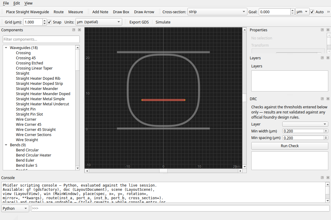
Reference GDS backdrop
File > Import Reference GDS… loads an existing layout (e.g. a foundry floorplan) to design against. It's shown dimmed and is not included in your own GDS export. It's purely a visual aid. File > Clear Reference removes it. The reference path is remembered with the saved project.
Design rule checking (DRC)
The DRC panel (right side) runs a width/spacing check against thresholds you enter yourself:

- Pick a layer.
- Enter a minimum width and/or minimum spacing in microns.
- Click Run Check.
- Double-click a violation in the results list to jump the canvas to it.
This checks against the numbers you typed in, not against any official foundry rule deck; the generic PDK this app uses doesn't ship one.
Saving, loading, and exporting
| Action | Menu | Produces |
|---|---|---|
| Save your editable project | File > Save / Save As | .phidler (JSON) |
| Reopen a project | File > Open | accepts .phidler or .py |
| Export final GDS | File > Export GDS | .gds |
| Export as Python code | File > Export Python Script… | .py |
.phidler is the full-fidelity project format: instances, routes,
layer colors, the reference backdrop path, and project settings all
round-trip exactly.
Unsaved changes are tracked the way most apps do it: the title bar shows the
file name with a modified marker (a leading *, or the standard edited dot on
macOS) whenever there's something unsaved, and it clears the moment you save.
Closing the window — or starting a New project or Opening another — with unsaved
changes prompts you to Save, Discard, or Cancel first, so you can't
lose work by reflex.
Exported .py scripts recreate your design with direct gdsfactory
calls (gf.get_component(...), add_ref, route_single). They're useful for
keeping a design as reviewable, version-controlled code. Running the
script directly (python my_design.py) writes a .gds named after the
script next to it.
Opening a .py script (File > Open) reads the actual code back into
Phidler, including hand-edits. If you change length=10.0 to
length=25.0 directly in the script and reopen it, Phidler picks up your
edit. This is additive to .phidler, not a replacement: layer colors and
the reference backdrop don't have a representation in the script format
and reset to defaults when you open one. Restructuring the generated code
(loops, helper functions, heavily renamed variables) isn't supported and
will raise a clear error rather than silently guessing wrong.
Scripting console
The Console dock (bottom, toggle from the View menu) is a Python REPL running against your live session:

Available names:
| Name | What it is |
|---|---|
gf |
the gdsfactory module |
doc |
the current LayoutDocument |
scene |
the current LayoutScene |
view |
the current LayoutView |
win |
the main window |
place(spec, x=, y=, rotation=, mirror=, **kwargs) |
places a component immediately |
route(inst_a, port_a, inst_b, port_b, cross_section=) |
routes between two ports immediately |
Multi-line blocks (for, if, def, ...) work like a normal REPL: keep
typing until you enter a blank line. Up/Down arrows recall history.
place() and route() are undoable: a single Ctrl+Z reverts a whole
console entry (a one-liner, or a for-loop that placed twenty things) as one
step, the same as any toolbar edit. Reaching into doc/scene directly still
applies immediately but bypasses undo — that's the power-user escape hatch.
Ask Claude to build it
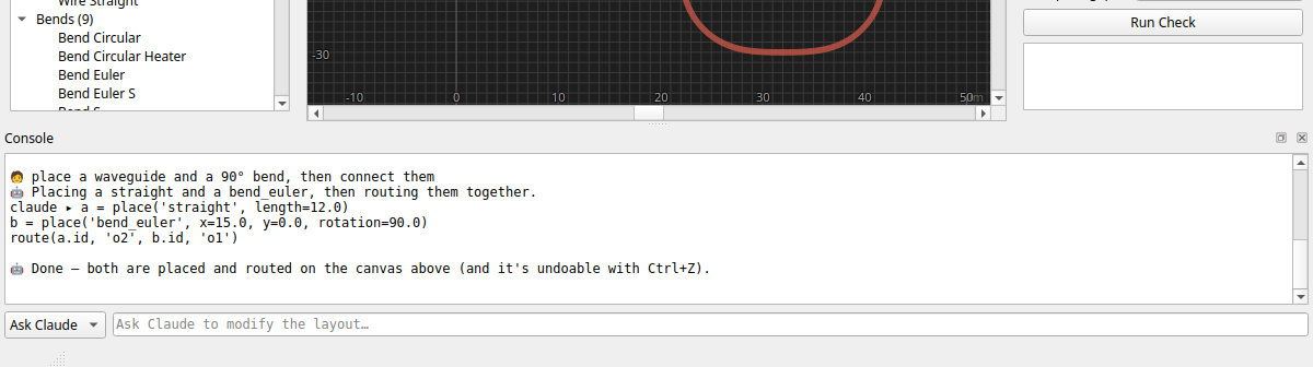
The scripting console is for when you'd rather type code than click. This is for when you'd rather just say what you want. Flip the dropdown at the bottom of the Console dock from Python to Ask Claude, type a request in plain English — say, "add a 2×2 MMI at the origin and route both of its outputs to the grating couplers on the right" — and Claude lays it out on the canvas while you watch.
It's optional. The mode only shows up when two pieces are in place: the ai
extra (pip install -e ".[ai]") and the Claude Code
command-line tool (claude) on your PATH. If either is missing, the dropdown
never appears and the Console stays an ordinary Python console.
Here's the part worth understanding: Claude doesn't get a separate back door into
your design. It drives the very same place() / route() / doc session the
console already gives you. So every edit it makes shows up right there in the
console, tagged claude ▸, and on the canvas — exactly as if you'd typed it
yourself. Nothing happens that you can't see scroll past.
A few things that make it feel less like talking to a black box:
- It knows what you've selected. Select two components and say "route these together," or select one and say "make this 3 µm longer" — Claude checks your canvas selection before it does anything, so "this" and "these" mean what you'd expect.
- You can ask, not just tell. "What's placed right now?" or "which ports does instance 4 have?" work fine; it reads the live document to answer.
- It stays in its lane. The bridge Claude talks to runs inside the app, on localhost only, and it's handed nothing but Phidler's own tools — placing, routing, running code in the console. It can't reach files on your disk or run shell commands through this.
Its edits are undoable, and grouped: one Ctrl+Z reverts everything a single Claude message did (all the components it placed and routes it drew), so you can let it draft freely and back the whole thing out in one step if it's not what you wanted.
FDTD simulation
The Simulate button in the toolbar opens a separate window that runs a
real local FDTD solve against your actual placed layout, using photonfdtd,
a separate, optional dependency not published on PyPI. If it's not
installed, you'll see a message explaining what to install instead of a
crash. The window has two tabs: a fast Vertical Mode Profile solver,
and full Propagation (FDTD) with movie playback.
Checking your cladding is thick enough
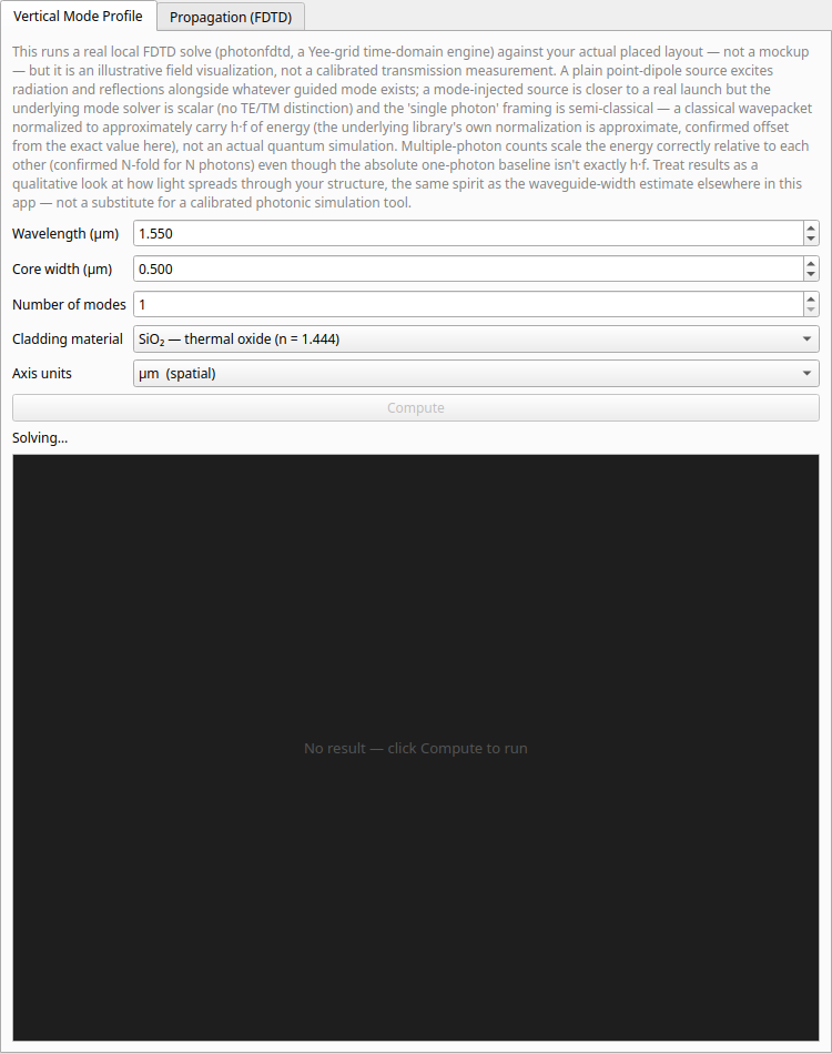
Before running a full simulation, the Vertical Mode Profile tab is worth a quick check. It solves the guided mode for your waveguide's cross-section in well under a second:
- Enter the Core width, Wavelength, and (optionally) more than one mode to solve for.
- Click Solve. The plot shows the mode's intensity confined within the core (outlined in cyan over the field), decaying into the cladding above and below.
- The status line reports the effective index and whether the mode is well confined or whether the cladding may be too thin. If your cladding (set in File > Project Settings…) isn't thick enough, the mode gets visibly squashed against the edge of the plot instead of decaying naturally. That's your answer to "is my cladding thickness enough" without needing a full propagation run.
Placing sources and running a simulation
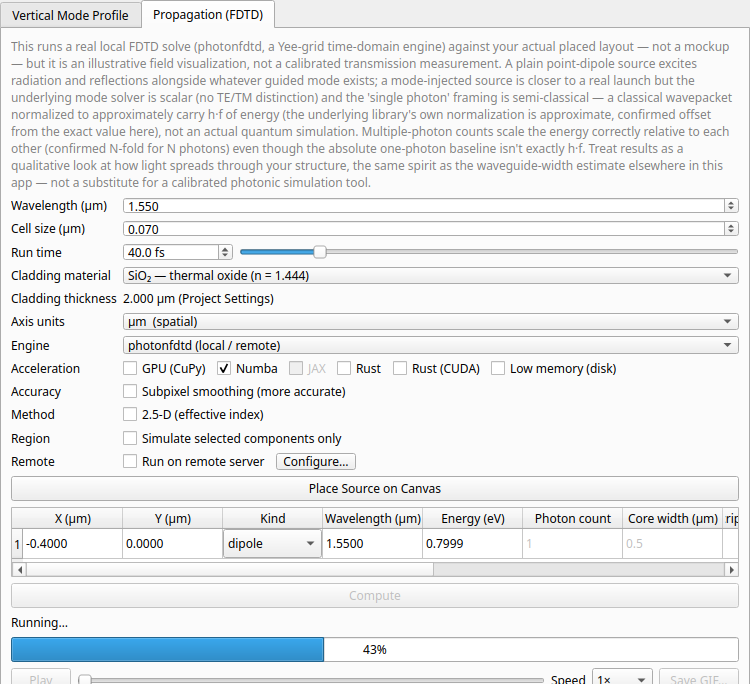
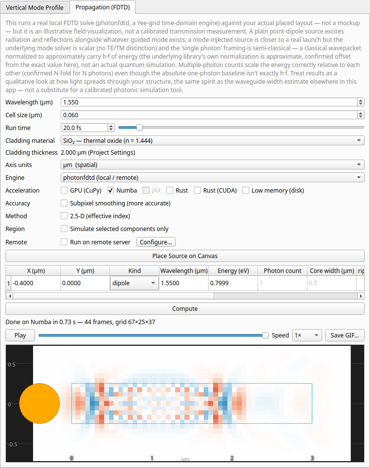
The Propagation (FDTD) tab runs a true 3D time-domain simulation and plays the result back as a movie:
- Click Place Source on Canvas, then click anywhere on the main canvas (clicking near a port snaps to its exact position, the same as the measure tool). Each click adds a row to the source table and a marker on the canvas.
- Set the source's color either as Wavelength (µm) or Energy (eV). Editing either column updates the other automatically, so you can specify "a photon at 0.8 eV" directly instead of converting it to a wavelength by hand.
- In the table, pick each source's Kind:
- dipole: a plain oscillating point source. Always available, simplest option, not mode-matched to anything.
- single_photon: launches a wavepacket built from the real guided mode at that position (needs Core width filled in), normalized to carry approximately one photon's worth of energy. Photon count scales the energy up from there.
- scripted: type a Python expression of
t(time, in seconds) into the Script column, e.g.np.sin(2*np.pi*1.93e14*t) * np.exp(-((t-3e-15)/1e-15)**2)(npis available). Evaluated with the same trust model as the scripting console elsewhere in this app: full Python, not a restricted sandbox, since this is already a single-user desktop tool. Wavelength/Energy/Photon count/Core width are ignored for this kind. - cherenkov: models a charged particle punching up through the chip (perpendicular to the layout plane, out of the top-down view) faster than light's local phase velocity. It is laid down as a track of point dipoles along the z axis, each fired with a delay equal to the particle's transit time to that point (distance / βc), whose superposition forms the Cherenkov shock cone, seen top-down as a ring spreading from the impact point. Set the particle speed β = v/c and the tilt from vertical in the source row (Cherenkov radiation requires β·n > 1, i.e. faster than the medium's phase velocity).
- Set Cell size and Run time, then click Run Simulation. If the estimated run time is more than a few seconds, you'll be asked to confirm first. True 3D propagation is genuinely more expensive than a quick preview, and this estimate is calibrated against real measured runs, not guessed. Run time goes up to 100 ps on the slider (1 ns if you type it into the box) for watching light propagate over a long distance; however long the run, the movie is kept to a few hundred frames so it stays playable.
- Once it finishes, use the Play button and the slider underneath to scrub through the field evolving over time, overlaid on a cyan outline of your actual chip layout, looping back to the start automatically. Speed sets the playback rate (0.25×–4×), and Save GIF… writes the whole animation (field plus chip outline, exactly as shown) to an animated GIF at the current speed.
While a run is in flight, a progress bar under the Compute button tracks it: a busy indicator during start-up (the kernel compile locally, or connect-and-upload for a remote run), then a 0–100 % fill as the solve steps through time. The same bar drives local, GPU, and remote runs.
Measuring intensity at a point
Sources tell you what goes in; measurement probes tell you what comes out at a particular spot — how much light actually reaches the far arm of a splitter, or how much survives a bend.
- Click Place Measurement Probe on Canvas, then click the point you want to measure. Clicking near a waveguide joint — any component or route port — snaps the probe to that joint exactly, the same snapping the source and measure tools use, so you can land on a connection point without pixel-hunting for it. Click well away from a joint and the probe stays exactly where you put it, which is what you want for a mid-span reading. Probes are green diamonds on the canvas, to tell them apart from the round orange source markers.
- Each click adds a row to the probe table reporting field intensity |Ez|² at that point: I (this frame) follows the playback slider as the movie plays, while ⟨I⟩ (run mean) and I (peak) summarise the whole run. The numbers are in the field's own arbitrary units — comparing probes with each other is meaningful, reading one as an absolute power is not.
- Probes are pure post-processing over the field movie the run already records, so they cost nothing to move and never require a re-run. Drop a probe after a simulation has finished and it fills in immediately; type new X/Y values into its row and it re-samples the same result at the new point.
A probe placed outside the simulated grid reads off grid rather than zero — most often a probe left over from a whole-layout run when you've since switched on Simulate selected components only.
Live intensity graphs
Each probe row has a Graph tick (on by default). While it's ticked, that probe's intensity-vs-time trace is drawn in the top-right of the field view in the probe's own colour, with a dashed playhead marking the frame on screen — so the graph animates in step with the field as you play or scrub.
The graphs can be exported two ways:
- As part of the sim canvas: they're painted into the field view itself, so Save GIF… writes them into the animation alongside the field and chip outline, playhead sweeping as the movie runs.
- Separately: Export Graphs… writes either a PNG of the graphs on their own (no field behind them) or a CSV of time in femtoseconds plus one intensity column per probe, for plotting elsewhere.
If the window is too short to stack every graph, the overlay says how many it had to hide; Export Graphs… always includes all of them.
Speed
Propagation runs use a few accelerators so they don't crawl:
- Numba (the Acceleration row) is on by default when installed. It JIT-compiles photonfdtd's field-update kernel (roughly 5× faster than the plain NumPy engine) and runs in the background, so the window stays responsive. The very first run compiles the kernel and is slower; that's cached to disk, so every run after is fast.
- JAX (the Acceleration row, shown when the
jaxpackage is installed) is the way to use the GPU as of photonfdtd 0.9. Tick it and, if JAX sees a GPU, the solve runs there through XLA; if not, it runs on the CPU. Either way it stays in the worker thread, so the window stays responsive. The first run traces and compiles the stepper (slower), then that's cached. The box reads JAX (GPU) when a GPU is visible; to get the GPU build, install a CUDA jax (e.g.pip install "jax[cuda12]"). It's exclusive of the GPU and Numba boxes, so ticking it clears those. - Rust (the Acceleration row) is photonfdtd 0.12's compiled CPU core.
It runs the whole time loop natively — fused field passes and ghost-zone
temporal blocking — measured here at about 17× plain NumPy (~2.5× Numba)
on a 6-million-cell grid, agreeing with the NumPy engine to float32 round-off.
There's no JIT warm-up, since it's already compiled, and it stores the
absorbing-boundary state compacted to the boundary itself, so it's also the
lowest-memory in-core backend. Unlike the others this isn't a
pip install: it's an extension built from photonfdtd's ownrust/directory (cargo build --release, then copy the library next to the package). Without it the box is simply disabled. - Rust (CUDA) is the same core on the GPU. The whole domain stays resident
in VRAM, and streams through the copy engines in tiles when it doesn't fit, so
it holds a far bigger grid on the GPU than the other GPU paths. Needs the
extension built with
--features cuda. One caveat: the availability check only asks whether a device is present, so if your driver is older than the toolchain the extension was built with, the box will be enabled but the run fails at start-up with photonfdtd's CUDA error — fall back to Rust or JAX if you see that. - GPU (CuPy) is the older GPU path, now deprecated in photonfdtd 0.9 in
favour of JAX. It still works if you have CuPy installed (the CUDA build,
pip install cupy-cuda12x, or the ROCm build for AMD,pip install cupy-rocm-5-0) and runs in a separate process so it can't freeze the app, but prefer JAX unless you specifically need CuPy. Whichever ran, the status line names it ("Done on GPU (CUDA)…" / "…on JAX…" / "…on Numba…"), so a request that quietly fell back to CPU is visible. - The propagation domain keeps only as much cladding as the mode's evanescent field actually needs (a few decay lengths, scaled by your platform's index contrast), rather than the full cladding the mode solver uses. That's a thinner z-stack and a much smaller, faster run, with no change to the top-down field you see. (Runs are also single-precision by default.)
- The recorded field movie keeps only the one component and the one horizontal plane (mid-core, z=0) the playback actually shows, not the whole 3D volume, typically ~90× less memory. The plane shown is mid-core height, where the guided mode is strongest.
A sharper run: subpixel smoothing
The Subpixel smoothing checkbox (the Accuracy row) turns on photonfdtd's anisotropic subpixel smoothing. Normally every grid cell is wholly one material or the other, so a slanted or curved edge comes out as a staircase. With smoothing on, cells that straddle an edge get a blended, direction-aware permittivity instead — the boundary lands where it actually is, not on the nearest cell wall. In practice that means a given cell size resolves your geometry more faithfully, which is often a cheaper way to clean up a result than shrinking the cell size everywhere. It works on the NumPy, GPU, and JAX backends (but not Numba or Rust, which ticking it will clear) and costs a little setup time before the run.
A much bigger run: 2.5-D (effective index)
Every option above makes the same simulation go faster. The 2.5-D (effective index) checkbox (the Method row) instead makes it a smaller simulation, which is usually the larger win by far.
A photonic layer is a thin core etched into an in-plane pattern. Rather than resolving that vertical stack cell by cell, 2.5-D solves the stack's guided mode once and collapses it into an effective index: the region under a waveguide gets one index, the etched surround another, and a rib layer's remaining slab its own in between. What's left is your chip plan view as a 2-D problem. The vertical axis goes from a full core-plus-cladding stack to a single cell, so the cell count drops by that whole factor — on the default Silicon platform, around 20× on a small device and far more on a real circuit. That's the difference between simulating a region of your layout and simulating the layout.
It composes with everything in the Acceleration row, so 2.5-D plus Rust is the fastest configuration available.
The catch is that it's an approximation: it assumes the vertical mode profile separates from the in-plane confinement. That holds very well for routing — bends, directional couplers, MZIs, interferometers, anything that guides light around the plane — and poorly for strongly three-dimensional behaviour, like an out-of-plane grating coupler or a deep sub-wavelength gap. Two consequences worth knowing:
- Cladding thickness has no effect on a 2.5-D run. The reduction has already consumed the stack, so that setting goes back to being inert on this path.
- Cherenkov sources aren't available, because a Cherenkov source is a track through the vertical stack — there's nothing left for it to cross. Phidler says so rather than quietly producing something. A single photon source does work: it matches the lateral mode of the reduced index map instead of the vertical cross-section.
Use 2.5-D to see how light moves through a circuit, then confirm anything strongly 3-D with a full run over a smaller region.
Running out of memory on a big layout
The solve itself (the field arrays it steps in time) scales with the number of grid cells (about 100 bytes per cell), and on one machine that's the only thing that determines peak memory, so the whole-chip grid is what runs you out of memory. Two things help:
- The "Large simulation" dialog now estimates the run before it starts: the grid's predicted memory (the number that OOMs) and the run time on each backend (Numba / GPU / plain NumPy). Read it. It tells you if a run won't fit.
- Simulate selected components only (the Region checkbox): select the device(s) you care about on the canvas, and the FDTD domain shrinks to just their bounding box (plus your sources). On a sprawling layout that's the difference between tens of GB and a couple; gigabytes → fits. It grids whole components, so it never cuts a device in half, but light leaving the region is absorbed at the edge, so use it for a local look at a device, not a through-circuit measurement. The memory/time estimate reflects the smaller region too.
If even a region is too big, a coarser cell size is the other lever (fewer cells in every dimension), at some cost in accuracy.
Running on a remote server
If this machine is slow, low on memory, or has no GPU, you can offload a run to another machine over SSH (a workstation or a GPU box) and get the field movie back, while the UI here stays responsive. Tick Run on remote server and click Configure…. Setup is a single step:
- Enter your SSH host: a
Hostentry from your~/.ssh/config. That's the only required field. Phidler shells out tossh/scp/rsyncand lets your SSH config and agent/keys handle authentication; it stores no passwords (key-based, non-interactive auth is required). - Pick the remote Acceleration, or leave it on Auto. Auto inspects the remote's GPU during setup and installs the ideal backend for it — JAX on an NVIDIA CUDA 12 box (the recommended GPU path; photonfdtd 0.9 runs JAX on the GPU through XLA), CuPy on CUDA 11 or an AMD/ROCm card, or plain CPU/Numba when there's no GPU — then remembers what it chose. You can also pin a specific one (CPU (Numba), GPU — JAX, GPU — CuPy). Either way it's the remote's hardware that matters, not this machine's.
- Click Connect && set up. That one button tests the connection, installs phidler + photonfdtd on the remote if they aren't there yet (a one-time step, streamed into the log), detects the remote's hardware and installs the ideal accelerator, verifies, and saves. Click it again any time; it only reinstalls when needed (or when you tick Force reinstall, e.g. after updating a package).
The install location is derived for you (a managed venv under ~/phidler-remote);
open Advanced only if you want to install into a specific directory or an
existing interpreter. After setup, ticking Run on remote server sends each
run to that host and brings the result back automatically. The progress bar fills
from the remote solve just as it does locally, and the result reports the backend
that actually ran, so a request the remote couldn't honour is visible.

The remote must be a POSIX host (Linux/macOS) reachable by key-based SSH.
Projects that place custom components (local .py files) can't be offloaded
(those files don't exist on the remote), and that case is reported as a clear
error rather than failing mid-run.
Running on Tidy3D (the cloud solver)
The Engine dropdown at the top of the run controls picks which FDTD solver
runs the propagation. The default is photonfdtd (everything above — local, the
acceleration options, or SSH). Switch it to Tidy3D (cloud) to run the same
layout on Flexcompute's Tidy3D instead: a
different engine, not just a different machine. Phidler builds a tidy3d.Simulation
from your placed geometry — the same core/cladding, waveguides, and source
positions — submits it to Tidy3D's cloud, and plays the returned field movie back
in the same window.

It's a separate, optional install and needs an account: pip install
"phidler[tidy3d]", then configure your API key once with tidy3d configure (or
set TIDY3D_API_KEY). Until both are in place the Tidy3D option is greyed out
with a tooltip that says which piece is missing. A run consumes FlexCredits
from your Flexcompute account, so phidler asks you to confirm before submitting.
The Acceleration / Remote / Accuracy options don't apply on this engine (they're
photonfdtd's), so they grey out when Tidy3D is selected; Cell size, Run
time, Region, and your sources all still apply. This first version
supports dipole sources (the default); mode-matched / scripted / Cherenkov
sources aren't wired to Tidy3D yet.
Read the disclaimer in the window. Both tabs run a real solve against your geometry, not a mockup. But treat the results as a qualitative look at how light spreads through your structure, not a calibrated transmission measurement or an actual quantum simulation, the same spirit as the waveguide-width estimate in Project Settings. The mode solver is scalar (no TE/TM distinction), and "photon count" scales energy correctly relative to itself, but the absolute one-photon baseline isn't exactly h·f; see the window's own disclaimer text for specifics.
The material stack (core/cladding index, core thickness, and now cladding thickness) comes from your current Project Settings platform. Switching between Silicon, SiN, LN, or LT there changes what gets simulated here too.
Rib waveguides (etch / slab layers)
By default the simulation treats the waveguide layer (1, 0) as a full-height strip and everything else as cladding. If your design uses a partial-etch slab (a rib waveguide, where a layer like SLAB150 (2, 0) leaves a thinner slab of core material beside the full-height ridge), list that layer under Etch / slab layers in Project Settings with its slab thickness. Both the propagation run and the vertical mode solver then model the ridge-over-slab cross-section: core material up to the slab height in the slab region, full core height under the ridge. Without it, a rib is simulated as if it were fully etched (no slab), which changes the mode and the confinement. A configured layer that isn't actually drawn in the layout is skipped (it won't silently map the wrong geometry).