Noah Paladino — MIT Physics
KrIO
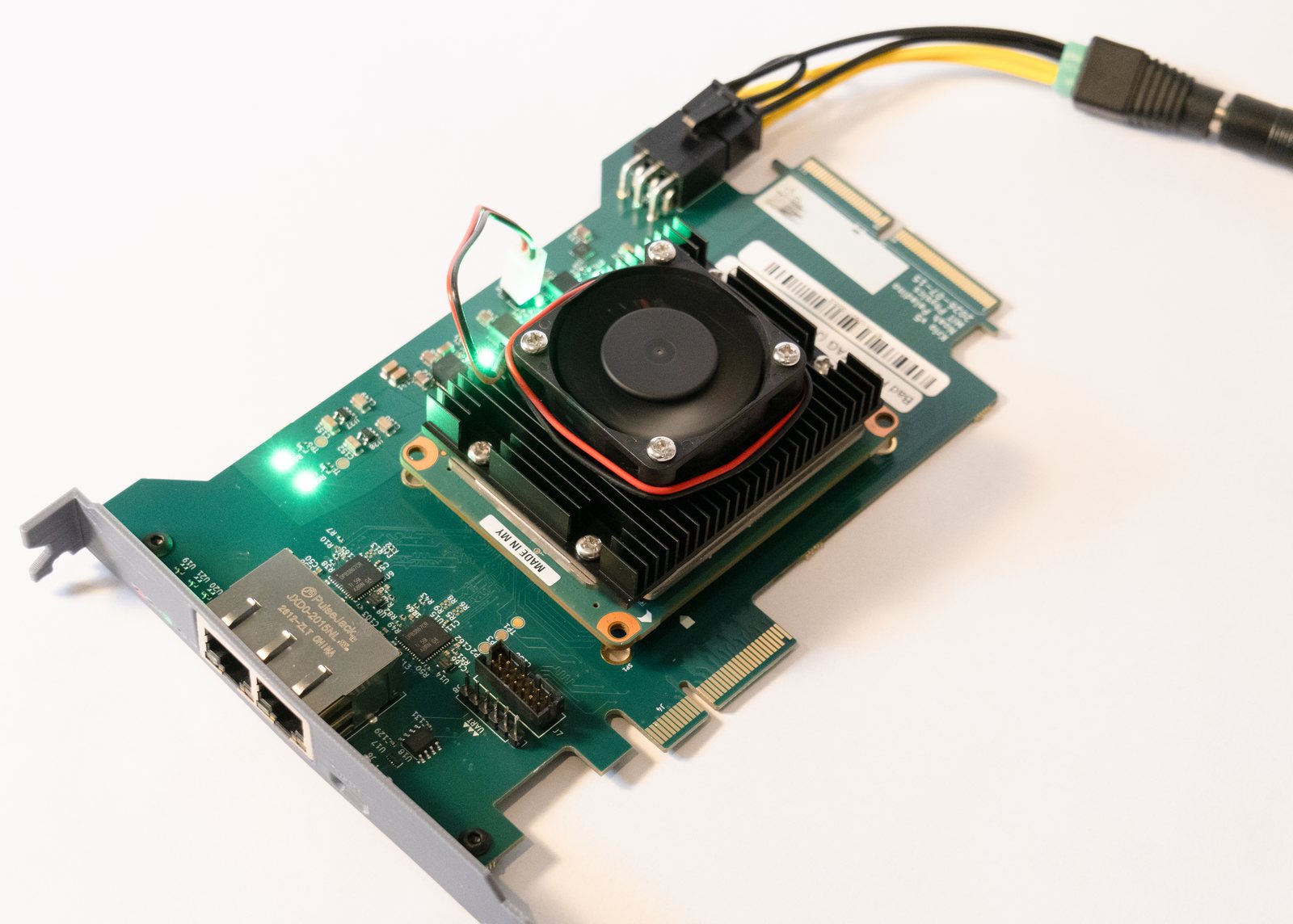
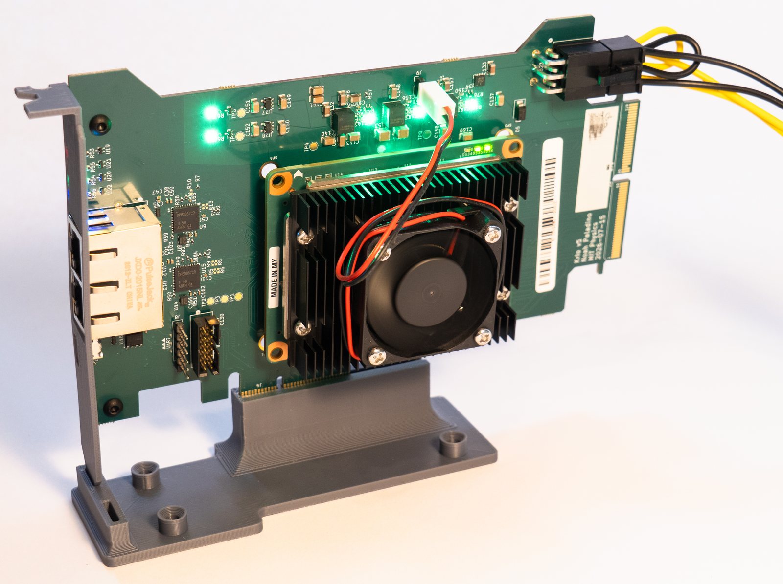
KrIO integrates an AMD/Xilinx Kria K26 module into a cost-effective platform that works with off-the-shelf systems while meeting the throughput demands of modern nuclear and particle physics experiments. Because the system is compact, flexible, and modular, it can be adapted to the data collection needs of a wide variety of scientific experiments.
The name is a portmanteau of Kria and I/O. The board gives the K26 68 channels of high-density I/O on a card edge, and sends real-time-processed data out over either PCI Express or Ethernet, the latter running up to 2 Gb/s across a bonded pair of gigabit ports, and it presents the same interface to every front end that plugs into it.
Why I built it
Nuclear and particle physics experiments suffer from the constant need for higher rates of detector data readout, processing, and collection to produce useful physics results. Older hardware cannot keep up, limiting the reach of experiments like SpinQuest. In addition, a lack of modularity within current solutions leaves researchers constantly reaching for a limited stock of spare components when things go wrong. A modular, open source DAQ platform using off-the-shelf parts allows for lower engineering costs, higher data collection rates, and better long-term availability of replacement parts, ultimately leading to more usable data and stronger results.
Every experiment I have worked on has built its own data acquisition hardware, and most of what gets built is not specific to the experiment. Clock distribution, transport, boot media, slow control, and the host interface are much the same whether the front end is a set of scintillator paddles, a silicon tracker, or a calorimeter, and in my experience they are the larger part of the effort. The parts that genuinely depend on the physics, primarily the analog conditioning and the digitizer, tend to be the smaller part, and they are the part people actually want to spend their time doing.
KrIO is my attempt to stop rebuilding the first category. Everything that does not change between experiments is on the module, and everything that does change sits on the other side of a Samtec HSEC8 card edge, on a board that can be a great deal simpler than it would otherwise need to be because it no longer has to carry a processor, a network stack, or a boot chain. Building it from off-the-shelf parts keeps engineering costs down and keeps replacement parts available over the long life of an experiment.
Already on the module
- Zynq UltraScale+ programmable logic and Arm cores, through the K26
- Linux, booting from QSPI flash or a 14.8 GB eMMC
- Two gigabit Ethernet ports, RGMII, bondable for up to 2 Gb/s
- A PCI Express x4 host link, as the alternative data path out
- Power tree, clocking, JTAG, and the whole boot chain
- Six layers with controlled impedance and the differential classes defined
Still yours to build
- The analog conditioning your detector needs
- The digitizer or discriminator, if the logic in the K26 is not enough
- One board carrying an HSEC8 socket to receive KrIO
- Your front end's firmware
The first front end I am building for it is a time-to-digital converter for SpinQuest, which is the origin of the initial pinout. In addition, the module is meant to serve later front ends without board changes, and the interfaces below were chosen with that in mind.
How it fits together
KrIO is the middle of three boards, and it is the only one of the three that gets reused unchanged.
Both J3 and J4 carry their own board outline, which is worth saying plainly because it decides who builds what: KrIO is the card, and the mating sockets belong to the front-end board and to the host.
What a front end has to provide
To use KrIO, an experiment needs one board with a Samtec HSEC8 socket on it. That board receives 68 high-density I/O signals arranged in three banks, and it does not need to provide a processor, a network interface, boot media, or a host connection, because all of those are already on the module.
| Signals | 68 single-ended lines to the K26's high-density I/O banks in three groups (HDA, HDB, HDC), plus six differential pairs on the high-performance bank |
|---|---|
| Connector | Samtec HSEC8, 2 × 60 positions at 0.8 mm pitch, edge-mounted |
| Pin map | All 120 pins are in the connector specification, generated from the KiCad project |
| Not required | Processor, Linux, PHY, QSPI, eMMC, PCIe — all on KrIO |
Because the assignment is bank-ordered rather than arbitrary, a front end can lay out its own connector without a crossing field on its side either. The full interface breakdown, including both transports out and where each one currently stands, is on the architecture page.
Documents
- Architecture§ 01
Connector by connector: what is fixed on the module, both transports out, and what each one currently demonstrates.
- KrIO Connector Specification§ 02
Every pin on J3 — the interface a front-end board has to meet, generated from the KiCad project and cross-checked between schematic and PCB.
- Board bring-up§ 03
Tutorial: power-on to running your own logic — boot images, console, network, and the rules this board imposes on anything you build for it.
- Running hls4ml§ 04
Tutorial: a trained Keras model to a firmware slot running on the board, with measured benchmarks for four models from the literature.
- Fabrication§ 05
Ordering from JLCPCB: the stackup the board is built to, generating the upload package, and the two specifications past the standard tier.
- Board errata§ 06
What bring-up on Rev 4 hardware proved broken, and what remains observed but not yet attributed to the board.
- Bill of materials ↗generated
Every line with its LCSC part number, regenerated from the schematic on each documentation build.
- Assembly & BOMgenerated
Every part cross-referenced against the board — click a row to find it on the PCB, or a part to find its row. Regenerated from the design on each build.
The board
From the design files
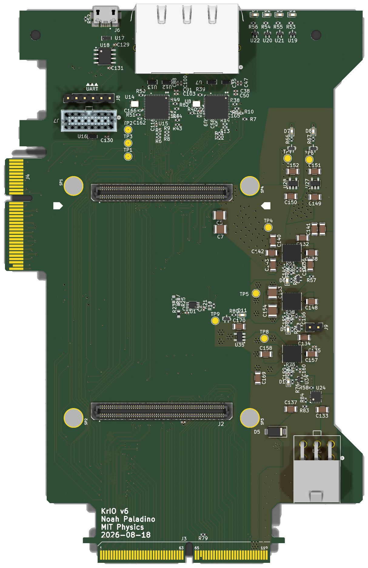
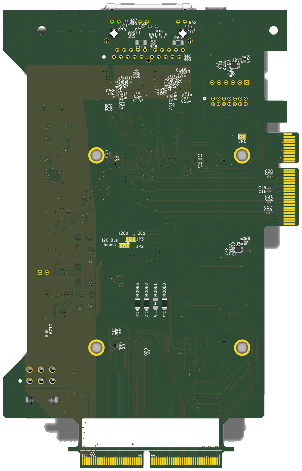
Both views are rendered from Krio.kicad_pcb on every
documentation build. Pin assignments for the front-end edge are on the
connector specification.